Learn More About Correlative XRM-FIB/SEM Workflow for Nanoscience

Advancing Correlative Studies in Nanomaterials and Nanoelectronics

  • Transform Your Sample Prep and Site-specific Analysis

    with Efficient Workflows

    Micro- and nanomaterials for electronic circuits and packages are critical to improve performance and reduce energy consumption. Continued miniaturization puts forward new requirements for packaging and moves into the nanometer range.  
    Parallel advances in FIB-SEM and 3D X-ray microscopy have radically changed sample preparation and analysis. This opens new capabilities for semiconductor research, development and failure analysis.

    On this page explore:

    • Correlative microscopy for micro- and nanoanalysis
    • Gain new insights for materials characterization & failure analysis
    • Expand your analytical opportunities

    Let's get started...
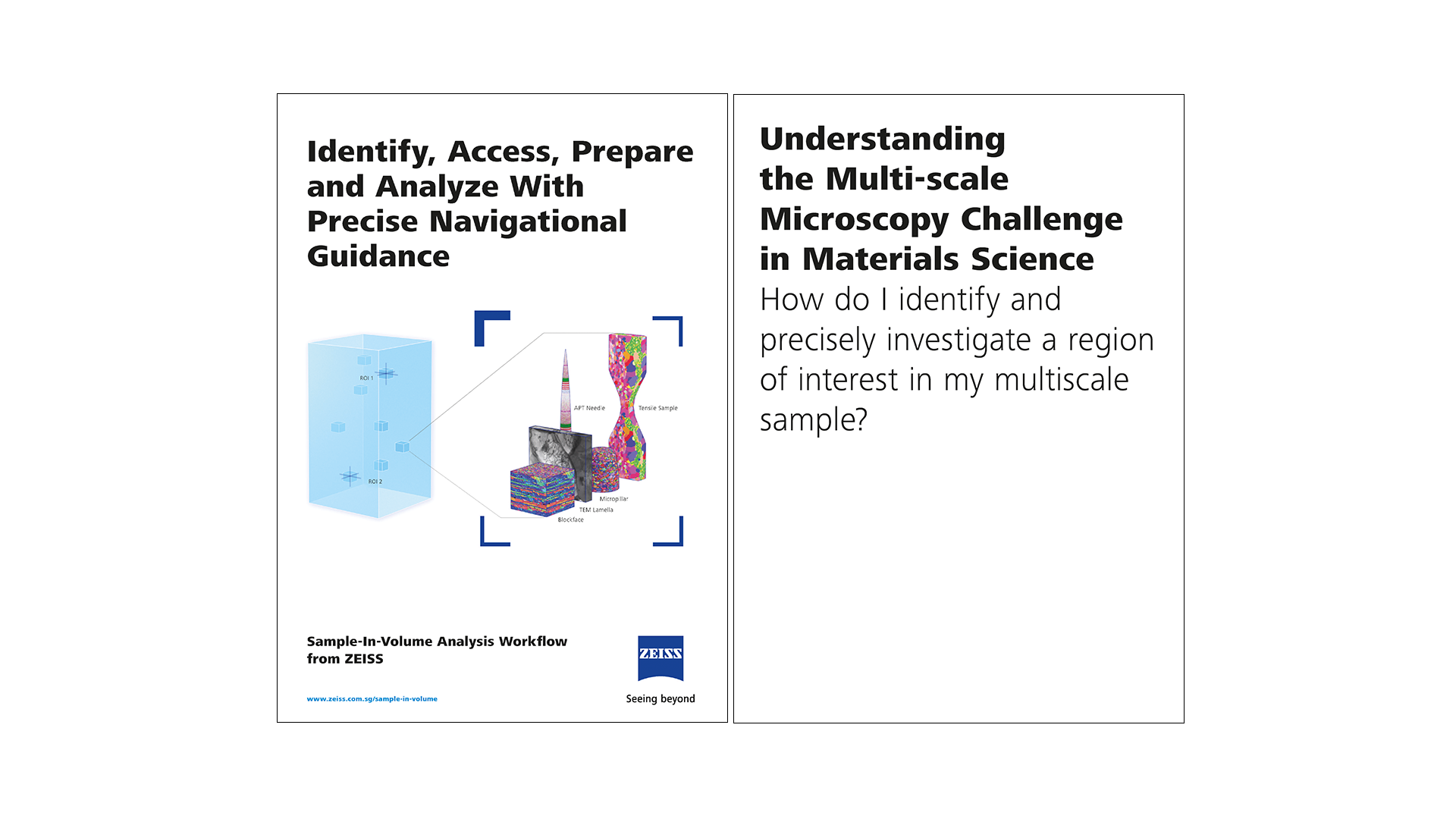
      

  • Identify
    Identify

    Identify your Region of Interest (ROI), Leaving your Sample Intact

    Achieve high-res imaging of intact samples.  

  • Access
    Access

    Expose the ROI in Your Sample

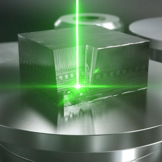
    Go from macro to nano in femtoseconds using a FIB-SEM with integrated fs-laser. Learn how to rapidly access buried interconnects in 3D packages with maximum speed and minimal artifacts.

  • Prepare
    Prepare

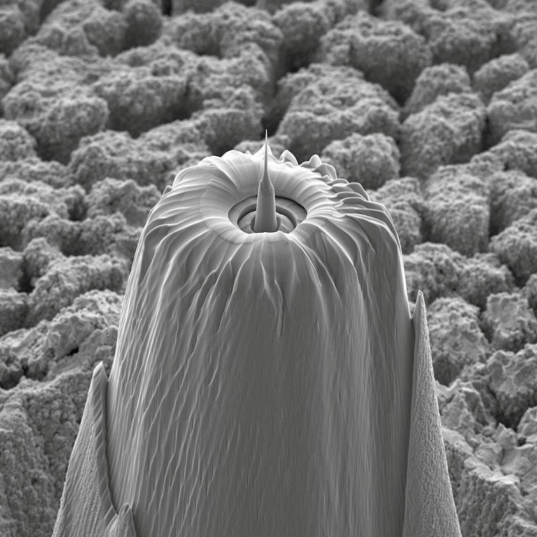
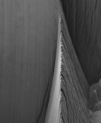
    Prepare Superior Quality Structures Using the GaFIB Column ZEISS Ion-Sculptor

    Minimize sample damage, maximize sample quality, prepare for experiments faster.  Remove cubic millimeters of material using fs-laser ablation and prepare your sample for the next step.

  • Analyze
    Analyze

    Fast Time to Result with Efficient Analysis

    Analyze and characterize prepared samples using a wide range of  analytical techniques including EDS, EBSD, ToF-SIMS, STEM, or in situ kits.

  • Explore ↓
    Explore ↓

    Discover the Workflow and Learn How to Find the Needle in the Haystack

    Explore correlative microscopy in a brief introduction below and learn more about the various areas of application.

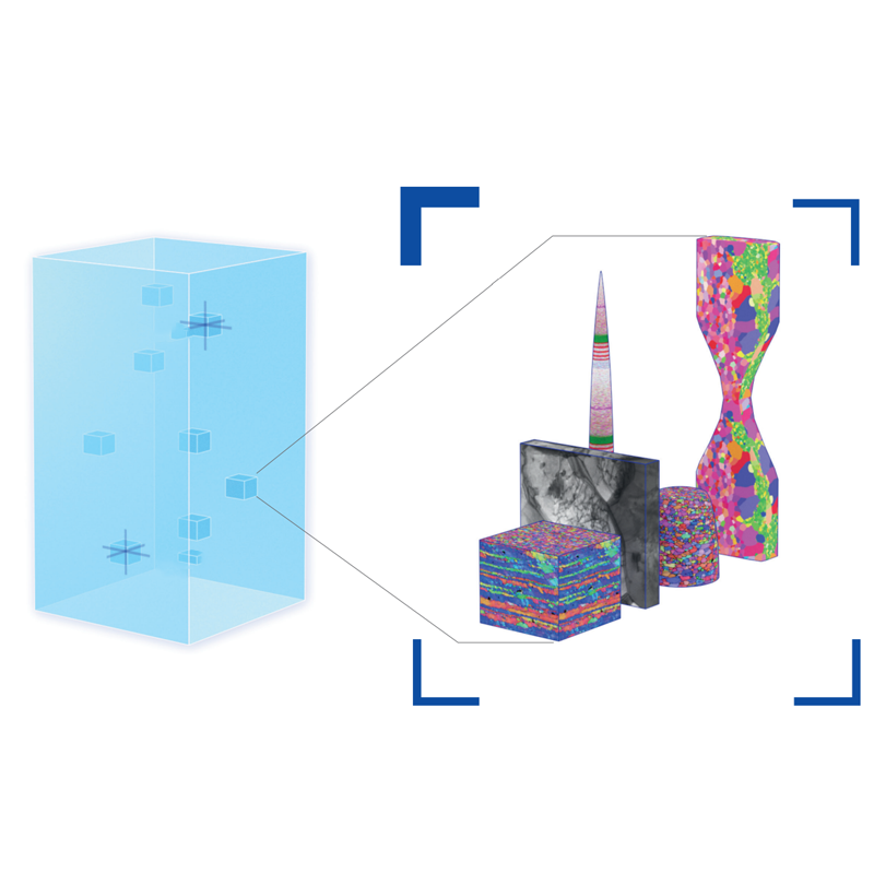
Solve the Multi-Scale Challenge

Sample in Volume Analyis

The Workflow in One Video

Finding the needle in the haystack explained in this video. Enjoy a brief introduction to lastest possibilities with correlative microscopy

FIB-SEM tomography dataset acquired from a commercially purchased 3D NAND sample.

Applications in Electronics & Semiconductor

Optimize your material for further production in the electronics area.  
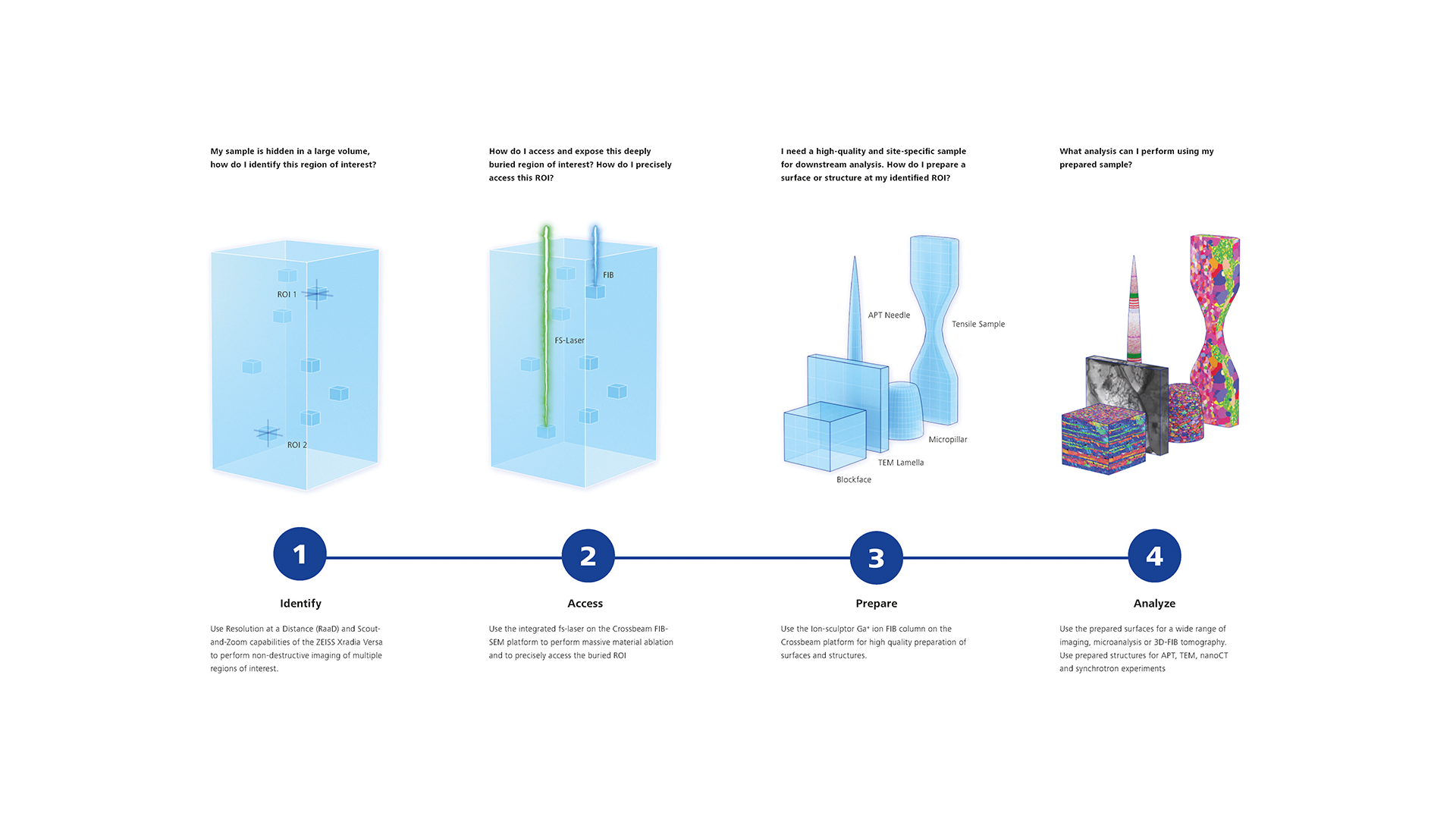
Learn more about Nanomaterials in Electronics & Semiconductor
Webinar 1

Advanced Package Analysis Solutions for the More-Than-Moore Era

The slowing of Moore’s Law continues to present challenges for integrated circuit (IC) package characterization and failure analysis (FA). Package developers and failure analysts are faced with complex System-in-Package (SiP) architectures enabled by heterogenous integration, package interconnect pitches approaching one micron, buried silicon and system-on-chip (SOC) disaggregation, leading to larger package footprints approaching 100mm x 100mm or larger. These trends drive requirements for new capabilities across the entire FA workflow. New ZEISS solutions addressing IC package analysis challenges will be presented including artificial intelligence for 3D X-ray imaging and a new “packaging FIB”, the ZEISS Crossbeam laser. These technologies represent significant advancements for the package FA workflow.

Webinar 2

Application of Ultra-Short Pulsed (USP) Lasers for Improved Microscopy Sample Preparation

A new instrument that integrates a femtosecond laser with a FIB-SEM (the LaserFIB) is revolutionizing sample preparation for microelectronics, as well as other industrial and research fields. Join this 1-hour webinar to learn about LaserFIB applications and understand how it compares to sample preparation tools such as broad ion beam (BIB), standalone ps-laser and integrated PFIB laser instruments.

Why Integrate a Laser with a GaFIB Instead of a PFIB?

Ga focused ion beams are cost effective and highly versatile: powerful enough today to polish a few hundred microns area, yet precise enough for 10 nm thick lamella preparation or 3D tomography with <5 nm isotropic voxel resolution. High quality fs-laser processing requires only minor FIB polishing at low currents, where a Ga beam has 35 times greater current density than a PFIB. This makes a GaFIB the most effective technology for the broadest range of applications.

Why Is an Integrated LaserFIB-SEM So Transformative?

The LaserFIB enables things that could never be done before, leading to higher productivity and new applications. Do you want 2X faster atom probe prep with higher sample quality than normal? Do you need to locate and image rare defects randomly distributed within a large volume? Do you need multiscale and multimodal analysis at timescales that enable statistical sampling for new material development? How about receiving large-area analytical results at unheard of speeds? This is just a small sampling of the new capabilities.

What Problem Is Addressed by an Integrated LaserFIB?

There is growing need for material and device characterization across length scales in microelectronics, battery research, and other industries. This includes a need to accurately perform nanoscale analysis, at site-specific regions contained within mm volumes of material, at faster rates than classical Ga and plasma FIB (PFIB) technologies allow.

Why Integrate a Femtosecond Laser into a FIB-SEM?

The LaserFIB architecture provides laser processing under vacuum conditions tailored for best quality, enabling rapid SEM imaging and visual feedback for process set-up and optimization. Laser integration enables automation and high productivity, while conserving floor space and cost of ownership.

Fresnel zone plate, example for nanopatterning.

Thin Films

Recent developments of nanotechnology have pushed the development of FE-SEMs and FIB-SEMs.

Caption:  Co nanoparticles embedded in  esoporous silica, STEM-EDS analysis, measured at 30 kV. High resolution EDS mapping of individual Co nanoparticles with approx. 10 nm size are resolved.

Learn More About Nanomaterials in The Area of Thin Films

ZnO Nanoparticles on a Carbon Film

STEM tilt series, brightfield STEM images are shown as one example of four signals collected in total simultaneously with the aSTEM detector using the special sample holder for STEM tomography. ZEISS GeminiSEM.    

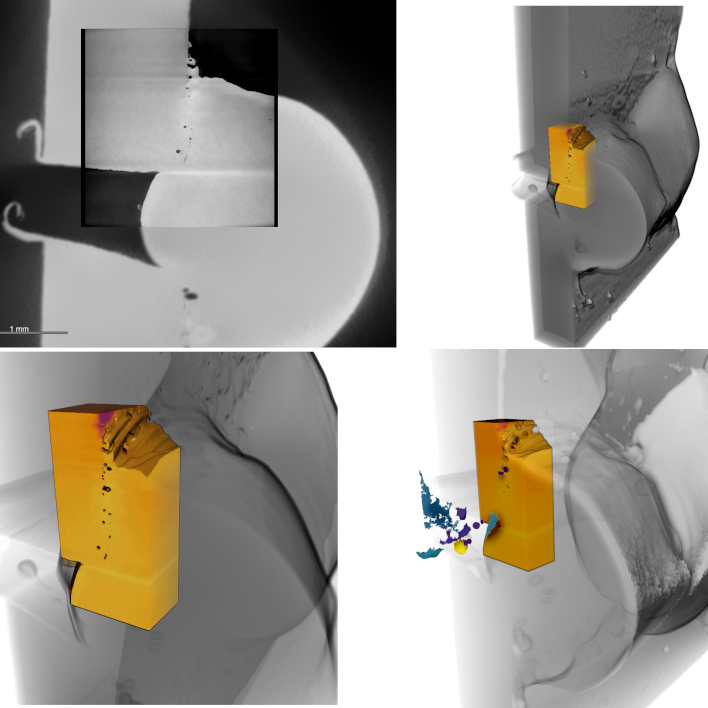
Trace Elements in Thin Films

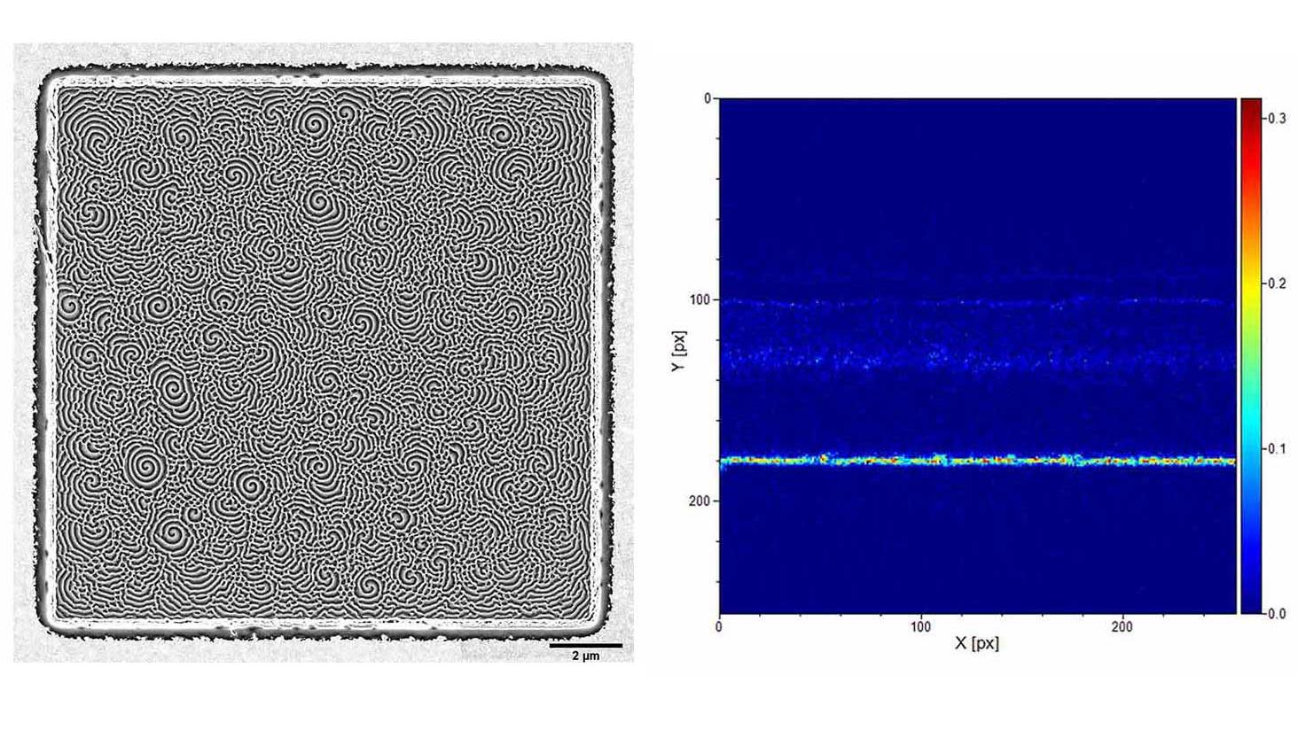
Perovskite solar cell on a glass substrate after a top-down SIMS measurement. ROI was scanned by the gallium beam 500 times. Secondary ions were analyzed spectroscopically according to their mass/charge ratio. A significant Na signal is observed across all layers. Intermixing and diffusion of trace elements can be studied by SIMS and is known to influence the performance of thin-film photovoltaic cells. (left SEM image, scale bar 2μm, right Na SIMS map). ZEISS Crossbeam 350 FIB-SEM with a Time of Flight (ToF) SIMS detector. Sample courtesy of Arafat Mahmud, RSEEME, Australian National University.

FIB-SEM tomography dataset acquired from a commercially purchased 3D NAND sample.

Photonics

Discover how an FE-SEM enables research on gold platelets used in sensors and how to prepare TEM samples easily with a FIB-SEM.

Learn More About Nanomaterials in The Area of Photonics
Webinar

Explore Photonics


Learn how to image and anlayze photonics samples with a ZEISS FE-SEM in this 20 min webinar.

TEM Sample Preparation

Step-by-Step Workflow Videos

  • Watch the workflow video and see all steps of a standard TEM sample preparation workflow with a FIB-SEM: how to locate and protect the region of interest, chunk the sample, cut it out, and perform the lift-out step in situ.
    How to prepare a standard TEM sample
  • To prepare a TEM sample in planar view geometry, locate and protect the region of interest before you perform cutout and liftout. Attach the sample to a grid lying horizontally, then flip the grid from horizontal to upright position.
    How to prepare a TEM sample in planar view geometry
  • To prepare a TEM sample in back side geometry, locate and protect the region of interest before you perform cutout and liftout. Attach the sample to a grid in upright position and perform various steps flipping and rotating the grid.
    How to prepare a TEM sample in back side geometry

Curious to learn more?

Sign up here to be one of the first, receiving exclusive educational material on Nanomaterials and receive a written summary of the above introduced Sample-In-Volume Analysis Workflow

Form is loading...

If you want to have more information on data processing at ZEISS please refer to our data privacy notice.

Take a Look Inside

  • Variable Pressure SEM with Optimized Low kV Imaging and EDS Analysis
    Variable Pressure SEM with Optimized Low kV Imaging and EDS Analysis

Share this Page