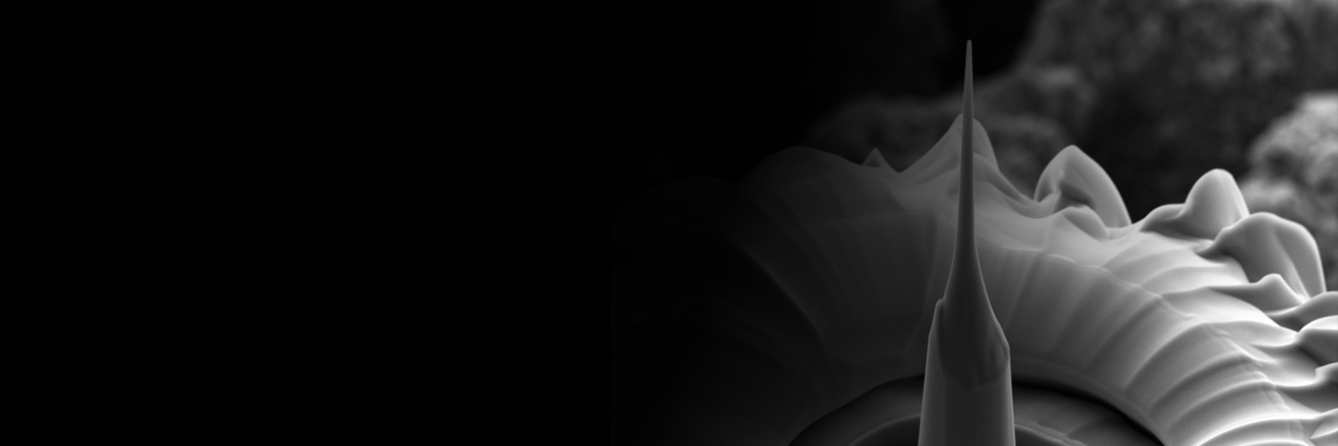

Of Needles and Haystacks
Advancing Correlative Studies in Materials Research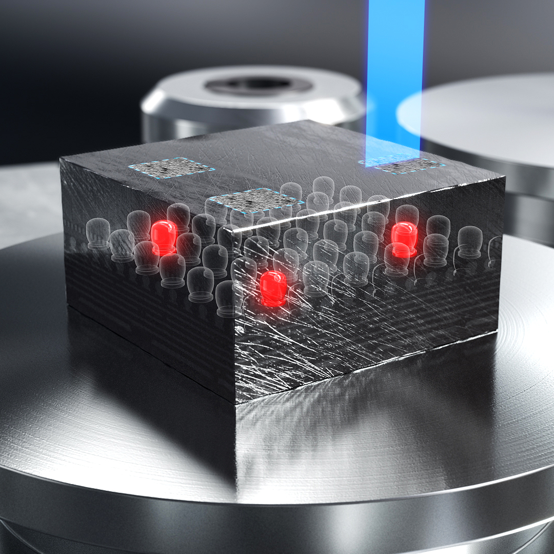

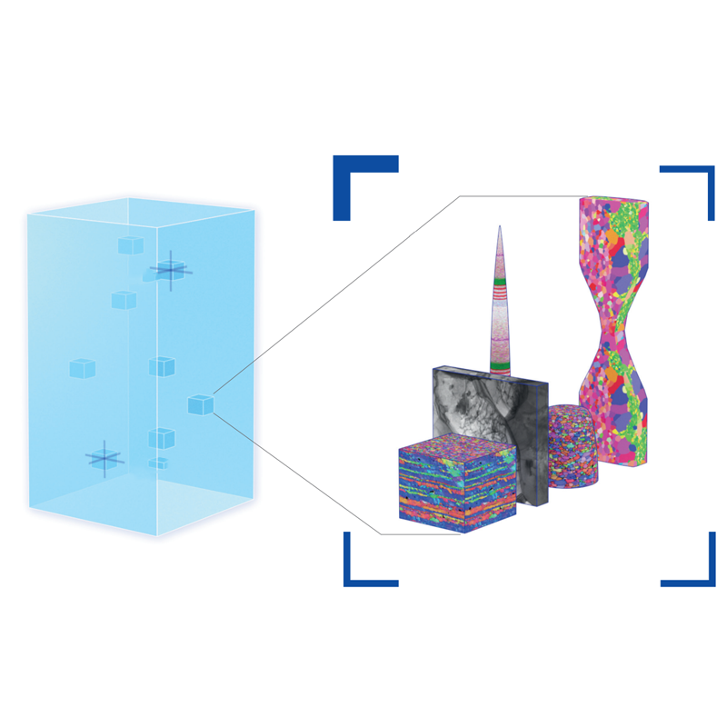
Target multiple ROIs
With High Accuracy and SpeedAccess regions of interest (ROI) that are hidden under the surface directly, revealing all structural details in a wide range of material types. Whether a hard or soft material, nanoscience, engineering or energy materials, conducting or insulating material: LaserFIB machines your sample at unprecedented speed.
Applications include cross-sections microstructural visualization and image analysis, various TEM sample preparations like extremely large H-bars, batch preparation of pillars e.g. titanium alloy for micromechanical testing or atom probe tomgraphy samples.
A LaserFIB, a combination of a ZEISS FIB-SEM and laser, enables you to localize ROIs in 3D, access deeply buried structures, ablate or process large volumes in a dedicated laser chamber, finalize preparation with the gallium beam of the FIB and do 3D imaging and analytics. Add a femtosecond laser to your ZEISS Crossbeam and benefit from ultrafast sample preparation.
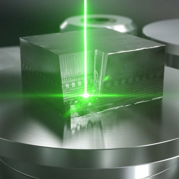

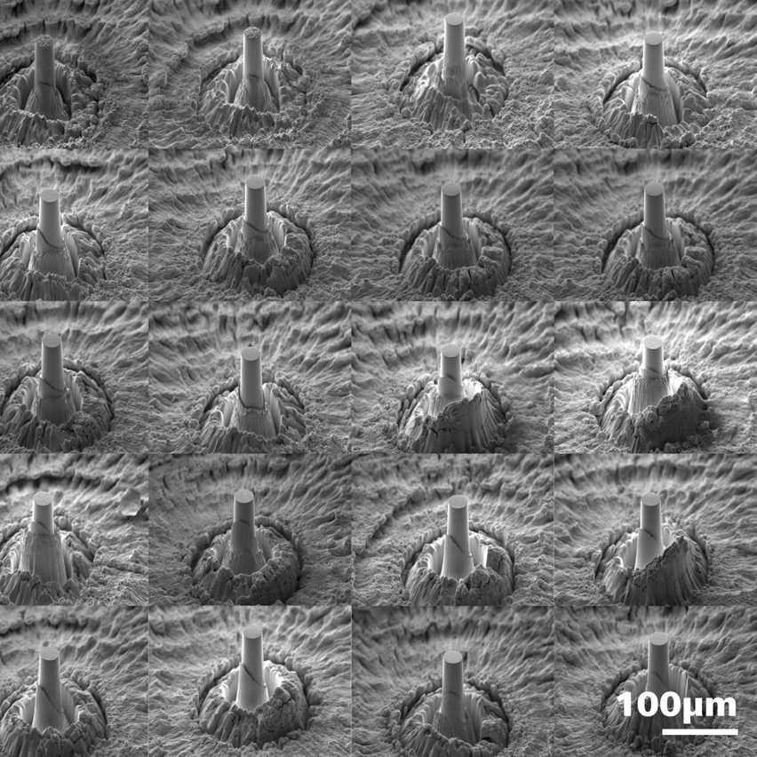
Massive Material Removal
Automatically Access Deeply Buried StructuresAutomated shuttling and laser processing in a separate chamber lets you save time and increase throughput, whilst scripting enables automated workflow creation, boosting efficiency in your experiments.
Thanks to the ultrashort pulse duration of the femtosecond laser, LaserFIB reaches highest removal rates of up to 15 mio. µm³ per second. These high ablation rates are ideal to prepare samples for further FIB machining with ZEISS Crossbeam, complementing LaserFIB with the highest precision at an even smaller scale (few nm – few 10 µm).
Watch the full LaserFIB Workflow Video
Discover Automation, Enhanced Throughput and Correlation


Execute Long-Term Automated Workflows
Ablate volumes of 10x10x10 mm3 without interruptionPerform laser processing in a dedicated chamber integrated to your LaserFIB and combine it with a tool that extends runtimes, enables consistent laser power and maintains ablation rates.
The new cross-jet, a gas flow of either nitrogen or argon, prevents ablated material to deposit on the protective glass under. This enables working for more than 8 hours continuously.


Prepare FIB-SEM Ready Structures
Polish and clean surfaces using the fs laserAutomatically polish and clean laser-cut surfaces using pre-installed recipes for various materials such as silicon or steel. Clean the surface of your sample of ablated debris with the laser beam. Transfer the sample automatically into the FIB-SEM chamber for further analytics.
Use the new Burst Mode to further increase ablation rates.
Learn more in 3 short presentations
and discover a workflow connecting XRM and LaserFIB, providing powerful, precise sample preparationExplore what the presentations will be about
Discover Advancing Correlative Studies in Materials Research Including Innovations in AI-Driven X-Ray & Laserfib 3D Microscopy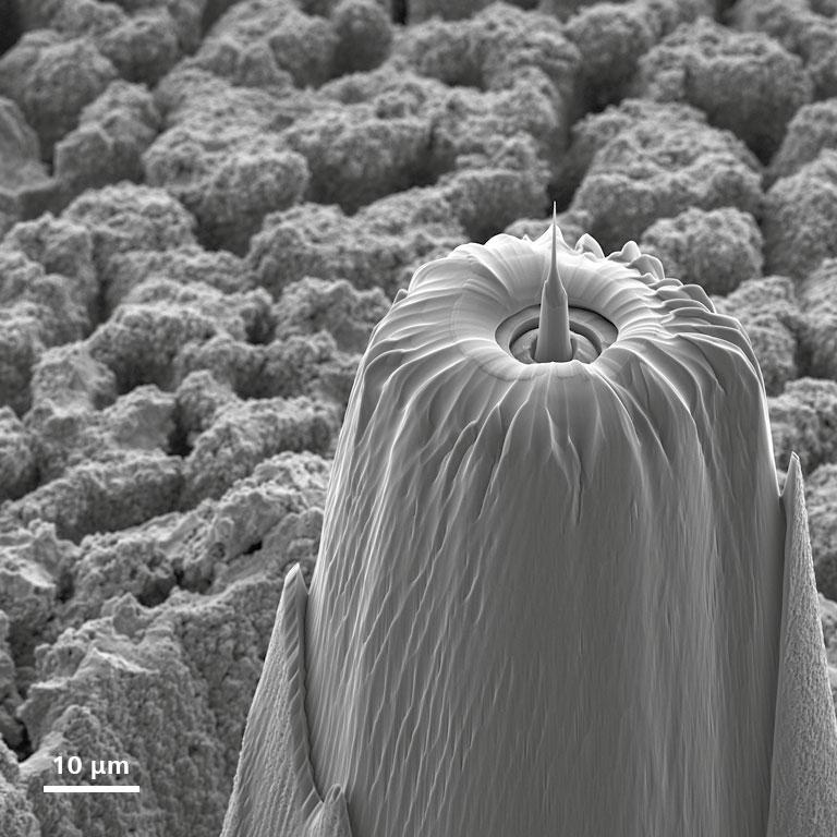


Stephen Kelly, Ph.D., is the Market Sector Manager for Energy Materials at ZEISS RMS. He has been working in the energy materials space for over 20 years and has extensive experience with materials characterization and fabrication across the energy materials space. He has been with ZEISS RMS since 2014.

Olena Vertsanova, Ph.D., is the Market Sector Manager for Nanoscience and Nanomaterials at ZEISS RMS since September 2022. After her Ph.D. in Solid-Sate Electronics in 2001 from the National Technical University of Ukraine (NTUU KPI) she has been working as Associate Professor at the Department of Micro- and Nanoelectronics of NTUU KPI. Her research interests were electron and photoacoustic microscopy, non-destructive testing, defects characterization, advanced semiconductor and new materials for nanoelectronics.

Hrishikesh Bale, Ph.D., is the Market Sector Manager for Engineering Materials at ZEISS RMS. He specializes in applications development for laboratory 3D X-ray imaging techniques. His research focus lies in 3D diffraction contrast tomography and in situ micro- and nano-mechanical testing using X-ray computed tomography. He has a strong background in materials science and mechanical engineering, with over a decade of experience in synchrotron X-ray microscopy and tomography.