Advanced Packaging Analysis Solutions
for the More-than-Moore Era

ZEISS Microscopy
Abstract
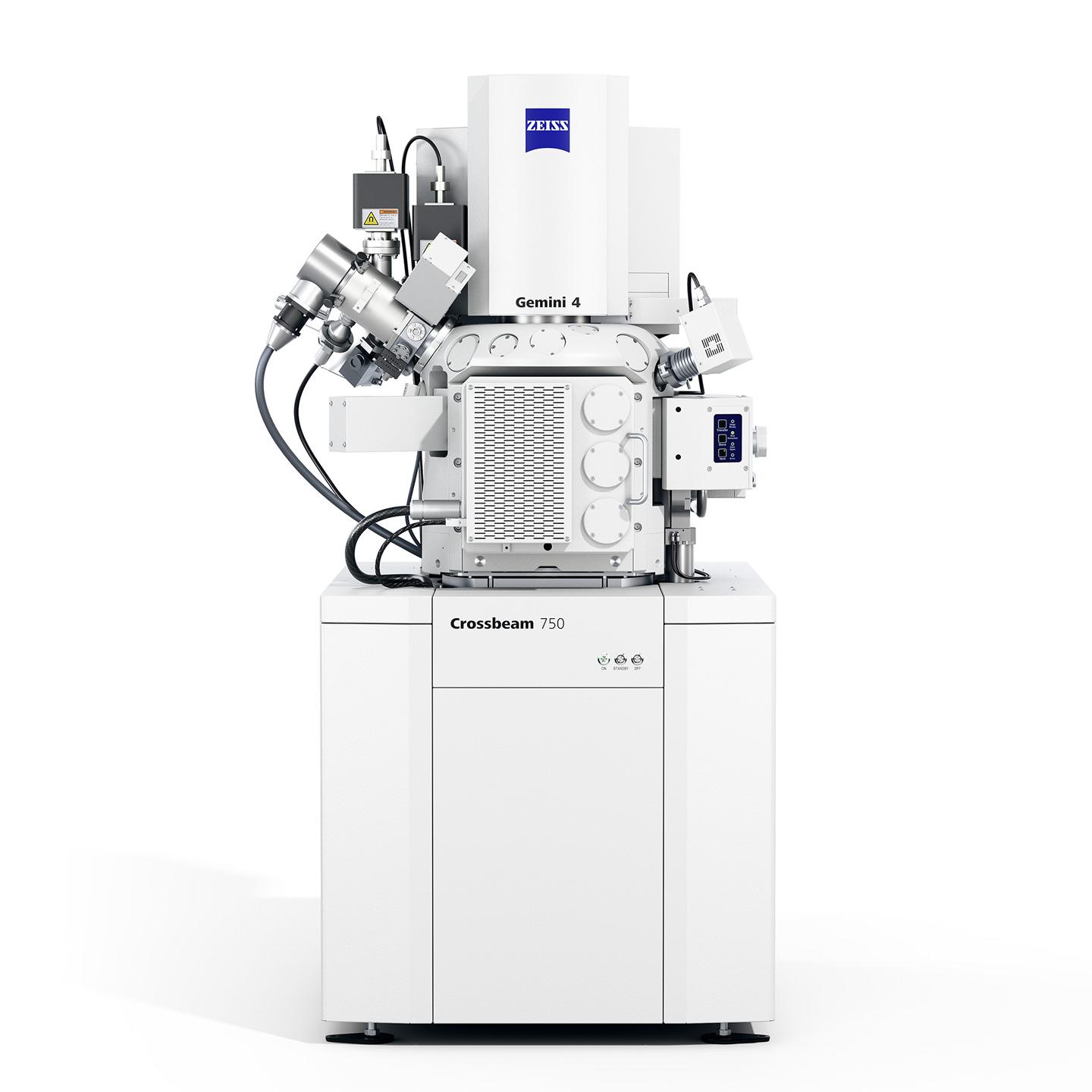
With the slowing of Moore’s Law, there has never been more urgency to address challenges for integrated circuit (IC) package characterization and failure analysis (FA) in the More than Moore (MtM) era. Diverse IC package strategies exist to enable the highest system performance. As a result, package developers and failure analysts are faced with complex package architectures, shrinking package interconnect pitches on the order of a few microns, and system-on-chip (SOC) disintegration, which leads to larger package footprints approaching 100mm x 100mm or larger. These trends drive requirements for new capabilities across the entire FA workflow. New ZEISS solutions addressing MtM IC package analysis challenges will be presented for 3D X-ray imaging and a new “packaging FIB”, the Crossbeam laser. These technologies represent significant advancements for the package FA workflow.
Key Learnings:
- An introduction to the "More-than-Moore" (MtM) packaging trend
- How 3D X-ray microscopy is used to address the challenge of MtM package analysis
- Technical highlights of a new "packaging FIB" for improvement of FA workflow