

Nanomaterials and Nanotechnology
Explore Properties of Nanomaterials with Advanced Microscopy Solutions
Innovation in nanotechnology is driven by increasing demand for cheaper and faster devices. To satisfy this demand, research into semiconductors, low-D materials, thin films, photonics and micro- and nanofluidics is becoming more complex. In other words, there is a constant drive to push nanosciences further so technology can advance beyond what’s currently available.
But nanomaterials research is only as good as the microscopy tools available. The right tools can help you easily gather critical information about your samples - and the more complex your sample or your research, the more stringent your analytical requirements will be. If your microscope cannot keep up with your research needs, then you and your project will be left behind.
Who used the term “nanotechnology” for the first time?
In 1974 the Japanese scientist Norio Taniguchi used the term “nanotechnology” to describe the precision manufacture of materials at the nanometer scale. However, the concept was first proposed by the physicist Richard Feynman in 1959. In his talk "There's Plenty of Room at the Bottom" he discussed the possibility of direct manipulation of individual atoms as a form of manufacturing though without using the term "nanotechnology" itself.


What are nanomaterials and how are they made?
Nanomaterials have at least one dimension that measures 100 nanometers or less. They possess unique properties, such as increased strength, chemical reactivity, or light sensitivity, compared to their larger-scale counterparts.
Top-down and bottom-up are two main approaches to create nanomaterials:
- Top-Down is a subtractive method, where larger bulk materials are reduced into nanoscale materials with physical or chemical methods e.g. milling, etching, or thermal decomposition. In the semiconductor industry, methods such as lithography are used to carve out nanoscale components.
- The bottom-up approach involves assembling atoms into nanoscale materials. Chemical reactions or self-assembly processes use molecules designed to spontaneously form the desired structure. Methods like chemical vapor deposition (CVD), atomic layer deposition (ALD), and molecular beam epitaxy (MBE) are common.
The required type of nanomaterial and its intended application determines the selection of the method. The bottom-up approach is often used in drug delivery, while the top-down approach is common for electronics or semiconductor.
What is the difference between nanoscience and nanotechnology?
Nanoscience and nanotechnology, though related, are two distinct fields that focus on the study and application of extremely small things.
- Nanoscience is primarily concerned with understanding the properties and behavior of materials at the nanoscale and devoted to the understanding of unique phenomena, including quantum mechanical effects and novel electrical, optical, and mechanical properties of materials.
- Nanotechnology leverages this understanding to design, synthetize, and characterize devices and create technologies for broad range of applications.


"What would you do if you could detect magnetic moments as small as 1 Bohr magneton? In fact, you could watch single electron spins flip. And that’s what we are trying to do with nanoSQUIDs - superconducting quantum interference devices. They consist of a ring intersected by Josephson junctions. They have ultrathin insulating tunnel barriers around one nm thick. We can fabricate SQUIDs with a ZEISS Orion Nanofab. As the junctions are small, TEM is needed on ultra-thin samples. The crystal damage can then be further investigated. Site-specific preparation, essential for the relocation of the regions of interest, can only be done with a FIB-SEM. To achieve atomic resolution, the thinnest high-quality samples are crucial."
Prepare a TEM Lamella and Investigate NanoSQUIDS
FAQ
-
Nanomaterials have unique and significantly different properties compared to their bulk counterparts due to their high surface area to volume ratio, and quantum effects. These properties can be categorized into physical, chemical, mechanical, magnetic, optical, and biological properties. They are: more reactive in catalysts; extremely strong; exhibit superparamagnetism which is useful for magnetic storage media or biosensors; quantum dots scatter light differently on the nanoscale; interact uniquely with biological systems making them invaluable for drug delivery, or imaging.
These properties can be tuned or controlled by altering the size, shape, and composition of the nanomaterials. As a result, nanomaterials have found applications in a variety of fields such as medicine, electronics, biomaterials, energy production, and environmental protection.
-
While nanoscience and nanotechnology hold great promise for innovation and improvement in many fields, they also present potential risks and challenges. These fall into primarily three categories. health and environmental risks, ethical and societal issues, and regulatory landscape. It's important to note that the scientific community is actively researching these potential risks and challenges. The goal is to understand and mitigate them, to ensure that the benefits of nanotechnology can be realized in a safe and responsible manner.
-
Microscopy plays a pivotal role in nanoscience by providing the ability to directly observe, characterize, and manipulate materials at the nanoscale. Techniques like SEM, TEM, and AFM offer insights into the atomic and molecular structures of nanomaterials, revealing their unique properties and behaviors, which are fundamental for advancing research and applications in nanotechnology.
-
A variety of instruments is used to synthesize, manipulate, and analyze materials at the nanoscale. Here are some key instruments:
- Scanning Electron Microscope (SEM) allow visualization at high magnifications and in high resolution.
- Transmission Electron Microscope (TEM): TEMs provide even higher resolution than SEMs and provide detailed information about the internal structure of nanomaterials.
- Scanning Probe Microscopy (SPM) includes Atomic Force Microscopy (AFM) and Scanning Tunneling Microscopy (STM), which can image surfaces at the atomic level and can also be used to manipulate individual atoms or molecules. AFMs deliver three-dimensional surface profiles and measure the force between a sharp probe tip and the sample surface.
- X-Ray Diffraction (XRD): XRD analyzes crystal structure.
- Spectroscopy techniques like X-ray Photoelectron Spectroscopy (XPS), Energy Dispersive X-ray Spectroscopy (EDX), and Fourier Transform Infrared Spectroscopy (FTIR) can provide information about the chemical composition and electronic structure of nanomaterials. Raman Spectroscopy is used to observe vibrational, rotational, and other low-frequency modes in a system, providing a structural fingerprint by which molecules can be identified.
-
Yes, certain microscopy techniques, such as energy-dispersive X-ray spectroscopy (EDX) coupled with SEM or TEM, can provide detailed information about the chemical composition of nanomaterials. These techniques allow for elemental analysis and mapping at the nanoscale, which is crucial for understanding the properties and behaviors of nanomaterials in various applications.
-
In nanoelectronics, microscopy is essential for the design, fabrication, and testing of components like transistors, wires, and circuits at the nanoscale. Techniques such as scanning tunneling microscopy (STM) and AFM can manipulate individual atoms and molecules to create electronic devices, while TEM and SEM are used to inspect the quality and structure of nano-electronic devices.
-
Microscopy techniques, especially those allowing for real-time interaction like AFM and STM, enable the precise manipulation of materials at the nanoscale. Researchers can use these tools to move individual atoms or molecules, construct nanostructures, and study the mechanical, electrical, and chemical properties of materials at the nanoscale, leading to novel nanotechnology applications.
-
Studying nanomaterials with microscopy presents challenges such as ensuring sample stability under high-energy beams, preparing samples without altering their native state, and interpreting data correctly due to the complex interactions at the nanoscale. Advanced microscopy techniques and careful sample preparation are crucial to overcoming these challenges.
-
Microscopy has been instrumental in advancing nanotechnology by enabling the visualization and analysis of nanostructures and devices, leading to innovations in electronics, materials science, and medicine. For example, the development of ultra-high-resolution electron microscopy has allowed scientists to observe the arrangement of atoms within materials, leading to the design of more efficient nanoscale devices.
-

Micromechanical Testing
-
Trace Elements in Thin Films
-
3D Analytics of Nano-materials
-

3D Printed Nanolattice Structure
-
CVD-grown MoS2 2D Crystals on Si/SiO2 Substrate
-
Structured Gold Platelets
-

3D Stacked Die Interconnec
-

Microfluidics Example


-

Micromechanical Testing
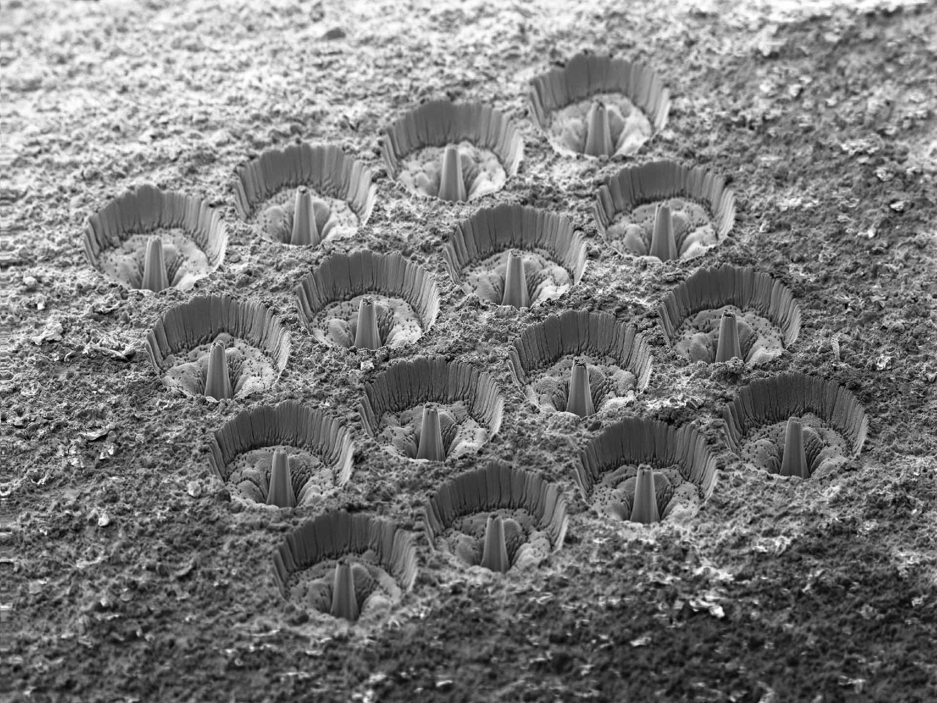
Pillar array machined using the fs-laser in a titanium alloy sample. These pillars could be used for micromechanical testing or as sample prep for X-ray microscopes after liftout. Size of each pillar: 100 µm tall, surrounded by 150 µm clearance on all sides, diameter at the tip 30 µm. Laser machining time for the whole array 2.5 mins. FOV 2.010 mm. ZEISS Crossbeam 350 laser -

Trace Elements in Thin Films
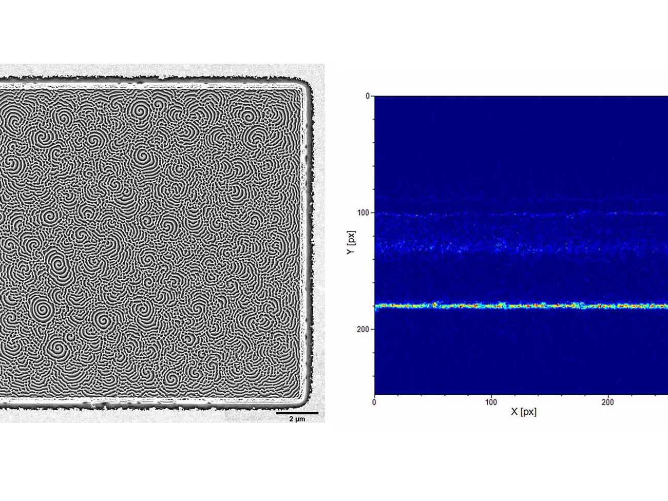
Perovskite solar cell on a glass substrate after a top-down SIMS measurement. ROI was scanned by the gallium beam 500 times. Secondary ions were analyzed spectroscopically according to their mass/charge ratio. A significant Na signal is observed across all layers. Intermixing and diffusion of trace elements can be studied by SIMS and is known to influence the performance of thin-film photovoltaic cells. (left SEM image, scale bar 2μm, right Na SIMS map). ZEISS Crossbeam 350 FIB-SEM with a Time of Flight (ToF) SIMS detector. Sample courtesy of Arafat Mahmud, RSEEME, Australian National University. -

3D Analytics of Nanomaterials
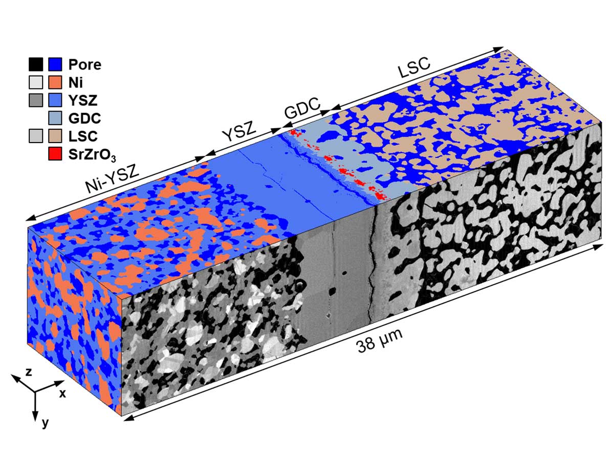
Microstructural degradation observed in a SOEC (Solid Oxide Electrolyzer Cell). 3D FIB-SEM/EDS enables the quantification of the extent of microstructural changes and detrimental effects on the cell performance. Compare: Characterization of SOECs by Advanced FIB-SEM Tomography, a ZEISS White Paper. ZEISS Crossbeam with EDS, ZEISS Atlas 5 with 3D Analytics module. Sample courtesy of M. Cantoni, EPFL, Lausanne, CH.
-

3D Printed Nanolattice Structure
Imaged in Zernike phase contrast before in situ compression experiments (sample width 30 µm). ZEISS Xradia Ultra. Sample courtesy: R. Schweiger, KIT, DE. -

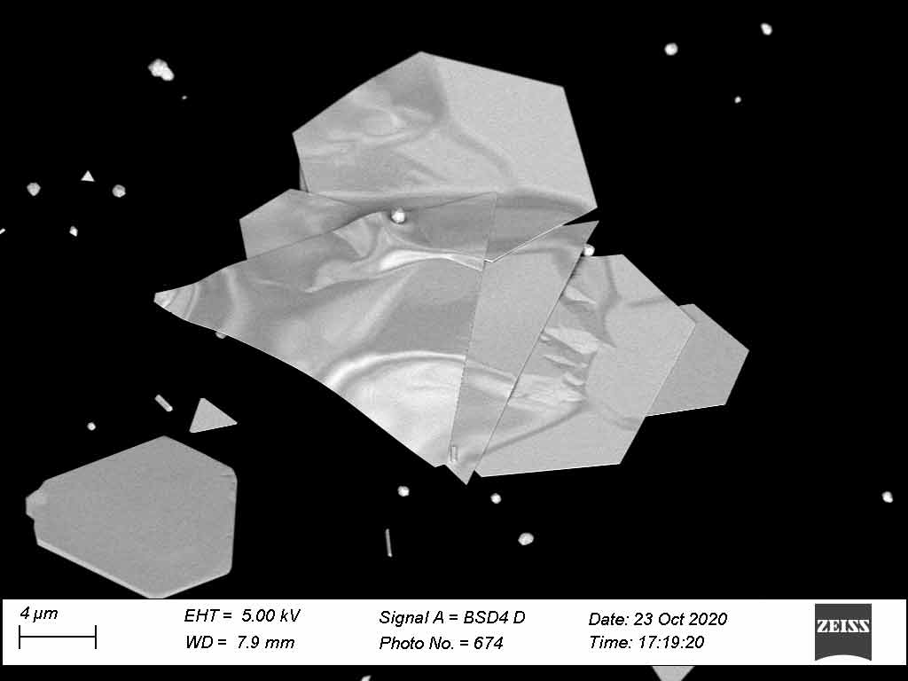
CVD-grown MoS2 2D crystals on Si/SiO2 substrate
The RISE (Raman Imaging and Scanning Electron Microscopy) image demonstrates wrinkles and overlapping parts of the MoS2 crystals (green), multilayers (blue) and single layers (red). ZEISS Sigma with RISE. Field of view 33 µm.
-

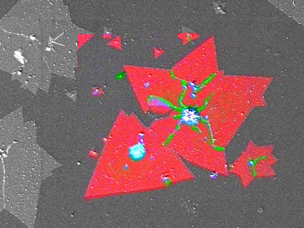
Structured Gold Platelets
Investigated as part of fundamental research on plasmonic effects.
ZEISS GeminiSEM 560. For more information compare: Science Advances 3, e1700721 (2017). Image: courtesy of University Stuttgart, 4th Physics Institute and Center for Applied Quantum Technology, Germany. Field of view 47.64 µm.
-

3D Stacked Die Interconnect
Cu-pillar microbumps buried 760 µm deep, cross-sections done in less than one hour. Field of view 2.58 mm, ZEISS Crossbeam laser.
-

Microfluidics Example
20 nm wide nano-channels in various configurations up to 20 μm in length. ZEISS Crossbeam & ZEISS Atlas 5 with NPVE module, field of view 59 μm.


STEM tilt series, brightfield STEM images are shown as one example of four signals collected in total simultaneously with the aSTEM detector using the special sample holder for STEM tomography. ZEISS GeminiSEM.
3D Tomography & Analytics
of a multi-layered metal system exemplified by a Canadian coin, typical FIB-SEM workflow combining milling, imaging, EBSD (top in this video) & EDS (bottom). Details, upper row from left to right: EBSD, copper, band contrast; EBSD, iron, Euler color; EBSD, nickel, IPF X. Lower row, from left to right: EDS maps of: copper, iron, nickel. ZEISS Crossbeam, ZEISS Atlas 5 with 3D Analytics module, EDS, EBSD.
Downloads
-
-

ZEISS Atlas 5
Characterization of Solid Oxide Electrolysis Cells by Advanced FIB-SEM Tomography
File size: 1 MB -

Achieving Nano-scaled EDS Analysis in an SEM
with a Detector for Transmission Scanning Electron Microscop
File size: 863 KB -

Targeted Sample Preparation with ZEISS Crossbeam laser
File size: 3 MB -

X-ray Nanotomography in the Laboratory
with ZEISS Xradia Ultra 3D X-ray Microscopes
File size: 6 MB -

FIB-SEM Fabrication of Atom Probe Specimens with ZEISS Crossbeam
File size: 1 MB -

Topography and Refractive Index Measurement
of a Sub-μm Transparent Film on an Electronic Chip by Correlation of Scanning Electron and Confocal Microscopy
File size: 1 MB
-


