
advanced microscopy techniques
Designing Lighter, Faster, and Stronger Engineering Materials
By revealing complex processing-structure-property relationshipsMicrostructural Imaging in the Metals R&D Lab


Recommended Products for Engineering Materials


ZEISS Research Essentials


What types of microscopy techniques are available for research of engineering materials?
ZEISS offers a variety of microscopy techniques tailored for materials design and engineering including:-
ZEISS offers a variety of microscopy techniques tailored for materials design and engineering including:
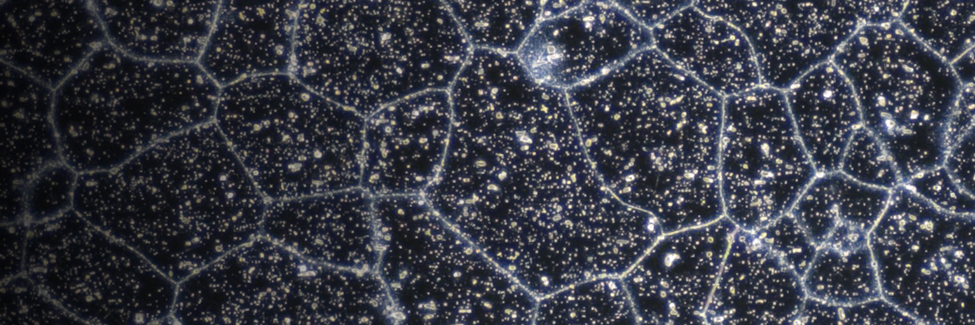
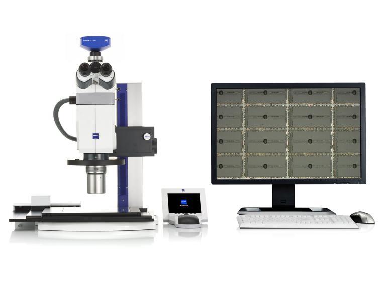
- Optical Microscopy: Addresses all typical metallography tasks using upright, inverted, zoom, digital, and confocal systems. Perform analysis of grain size, non-metallic inclusions, cast iron graphite, alloy multi-phase distributions, coating or layer thickness, surface roughness, or technical cleanliness.
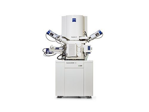
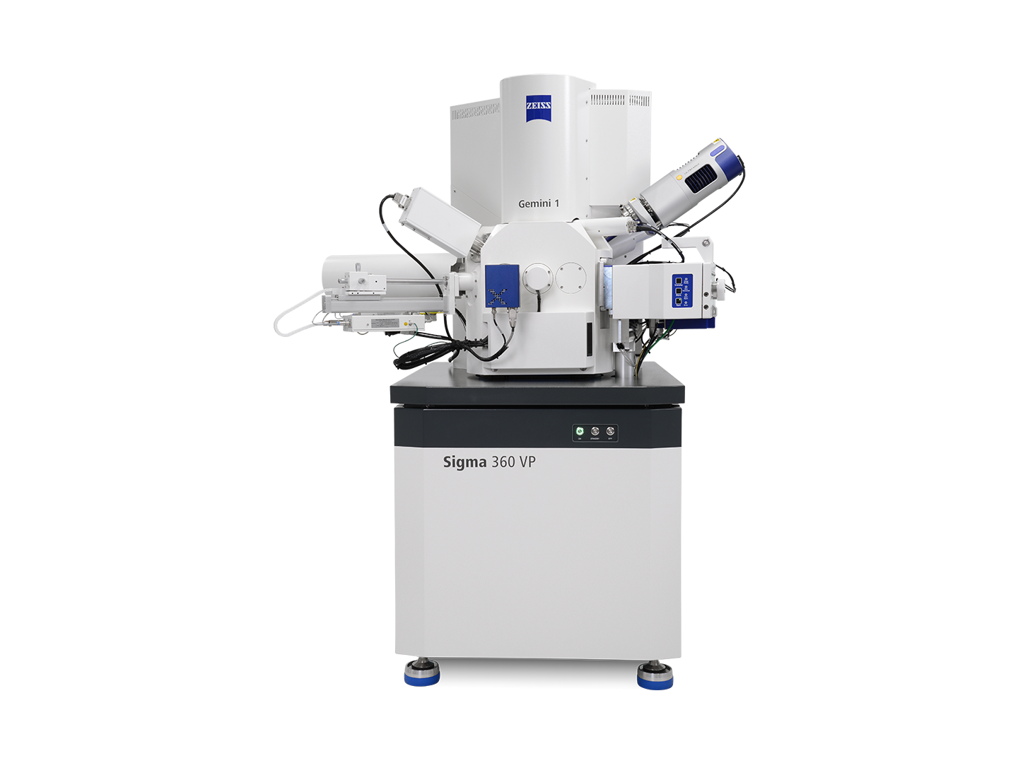
- Electron Microscopy: Provides ultra-high resolution for nanoscale visualization of material surfaces. Reveal precipitate phases, grain microstructures, crystal lattice defects and dislocations, chemical mapping, or perform automated in situ loading experiments.
- FIB-SEM Microscopy: Extends SEM analysis to the sub-surface with the addition of a gallium focused ion beam for targeted milling. Enables microscale sample preparation of pillars, dogbones, or TEM lamella, and also facilitates serial sectioning 3D tomography. By combining FIB-SEM with a femtosecond (fs) laser, researchers cover a huge range of material ablation demands.
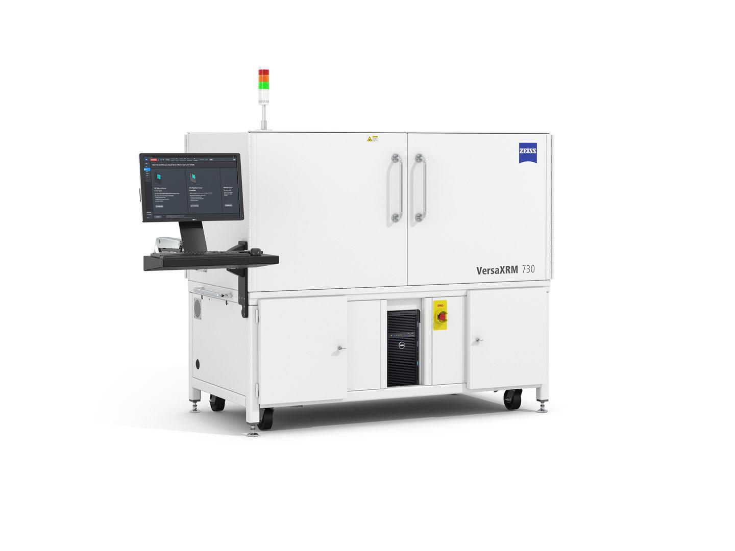
- 3D X-ray Microscopy: Delivers nondestructive 3D imaging by high resolution X-ray tomography. Perfect for analysis of internal sample features or morphology like voids, cracks, distributed particles, or crystalline microstructures.
These systems come together to form a versatile portfolio, empowering you to investigate the diverse range of features that exist within modern engineering materials.
-
The ZEISS microscopy portfolio is designed to address four key types of characterization challenges often faced by materials scientists:
- Routine Metallography: Fundamental characterization of metallic microstructures requires routine, efficient analysis of characteristics like grain sizes, phase distributions, and inclusion analysis. The different light microscope configurations from ZEISS, in combination with ZEN Core acquisition and analysis software, makes sure a researcher can perform these tasks easily, and in accordance with industry standards.
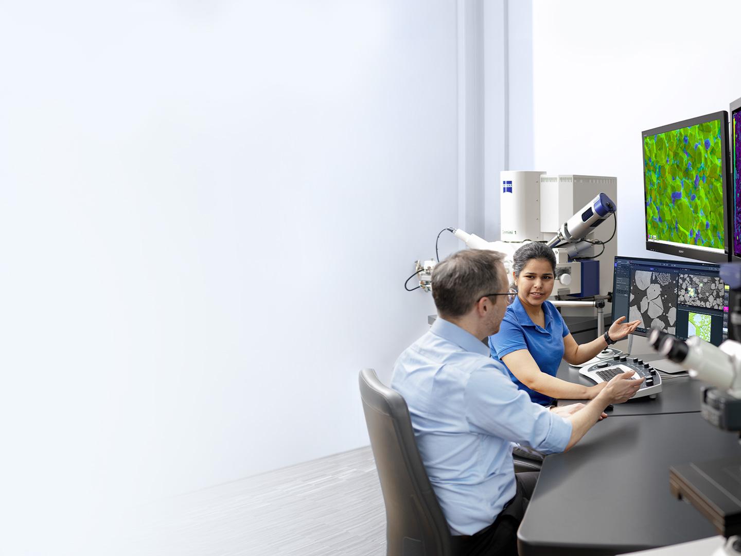
- Multiscale Imaging: Many engineering materials display hierarchical structures, with critical features spanning from the macro- to nano-scales. The extensive optical, electron, and X-ray portfolio of microscopes from ZEISS is designed not only to cover this range of needs, but help researchers connect their samples and image data to navigate through the different lengthscales and instruments in a coordinated and intelligent manner.
- 3D Characterization: The complex structures found in engineering materials usually exist in three dimensions, therefore it can be critical to work with imaging techniques that reflect and capture that complexity. ZEISS offers confocal laser scanning microscopy, 3D X-ray microscopy, and FIB-SEM tomography techniques to ensure materials’ structures are visible in all three spatial dimensions.
- In Situ Experiments: To best understand how a material will perform in a given application, scientists are often interested in observing how microstructures react under real operational conditions or under imposed stimulus/load. The ZEISS microscopy portfolio offers a variety of in situ experimental rigs and stages to easily facilitate such workflows.
-
The ZEISS microscopy portfolio addresses imaging needs across a broad range of material types:
- Metals & Alloys: ZEISS microscopes address the full range of characterization needs for metals and alloys research, from routine metallography to advanced 3D and in situ characterization.
- Composites: Composites, particularly fiber-reinforced polymer composites, are compelling alternatives to metallic materials, especially in weight-sensitive applications. X-ray microscopes from ZEISS, such as the VersaXRM, provide 3D images of fiber and matrix distributions that can be critical to understanding the unique, and sometimes highly anisotropic, 3D structures often found in these materials.
- Ceramics: ZEISS scanning electron microscopes, often in combination with focused ion beam, provide high resolution and surface sensitive imaging that is ideally suited to nano- and micro-scale features and grain sizes often seen in ceramic materials.
- Cementitious Building Materials: Concretes and similar building materials are critical for their high strength and low cost. Advanced imaging, such as with ZEISS 3D X-ray microscopy, can help better understand the connections between structure and mechanical properties, or even lead to advances in growing fields like self-healing materials.