

Expedite Complex Semiconductor Materials and Structures
With Accurate Failure Analysis
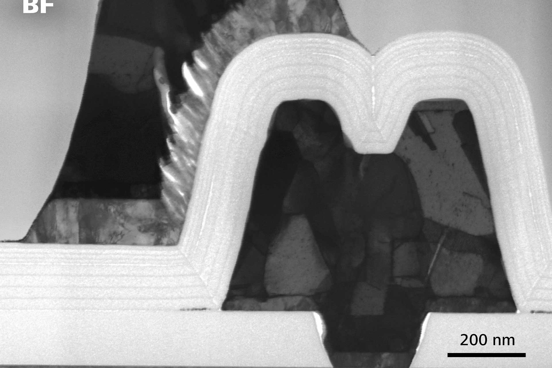

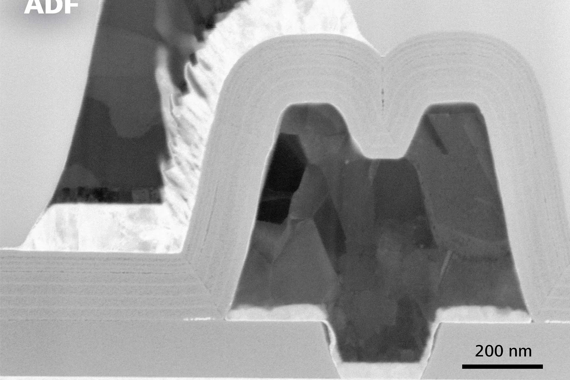

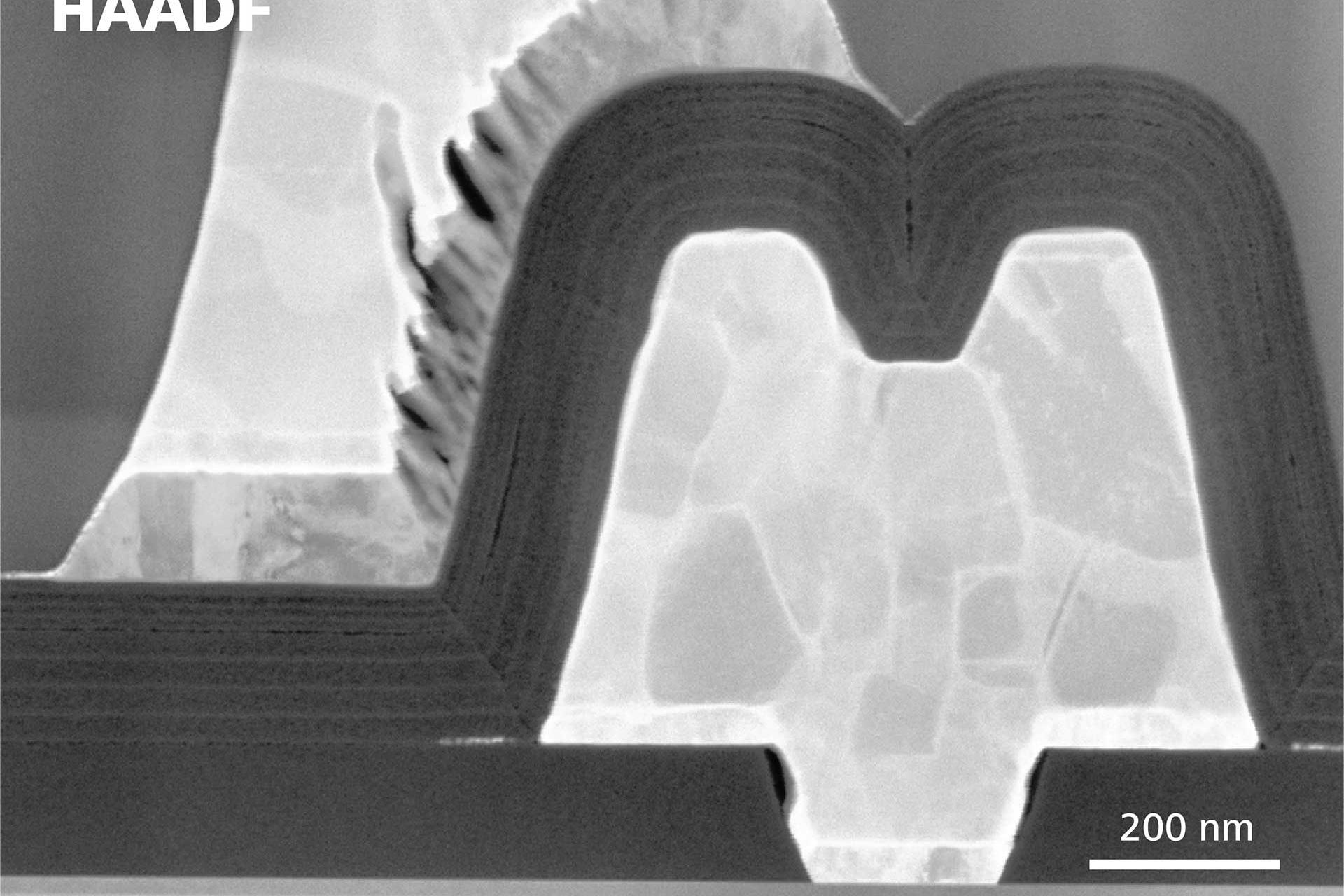

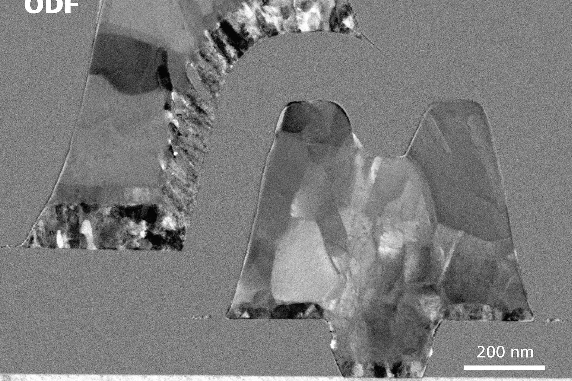


Cross Section and EDX of IGBT Device


Failure Analysis of IGBT Device
Microstructural and chemical examination of the edge of a gate in an Insulated Gate Bipolar Transistor (IGBT) device requires precise lamellae preparation and optimum EDS analysis.
ZEISS Crossbeam enables the complete workflow from lamellae preparation to STEM-in-SEM imaging to EDS analysis. Image showing correlative data, identifying crystalline Si precipitates.


Dopant Profile Image of SiC MOSFET


Voltage Contrast Imaging of Dopant Profile in a SiC MOSFET
Accurately determining semiconductor junction health and placement is important for performance of a SiC MOSFET device.
Cleaved SiC MOSFET device imaged at 1.5 kV in a ZEISS SEM. The image strongly highlights different implant doping regions due to the difference in work functions. The N+ diffusion is shown as a dark band underneath and extending to either side of the gate. The P-type body region is highlighted as a bright zone.
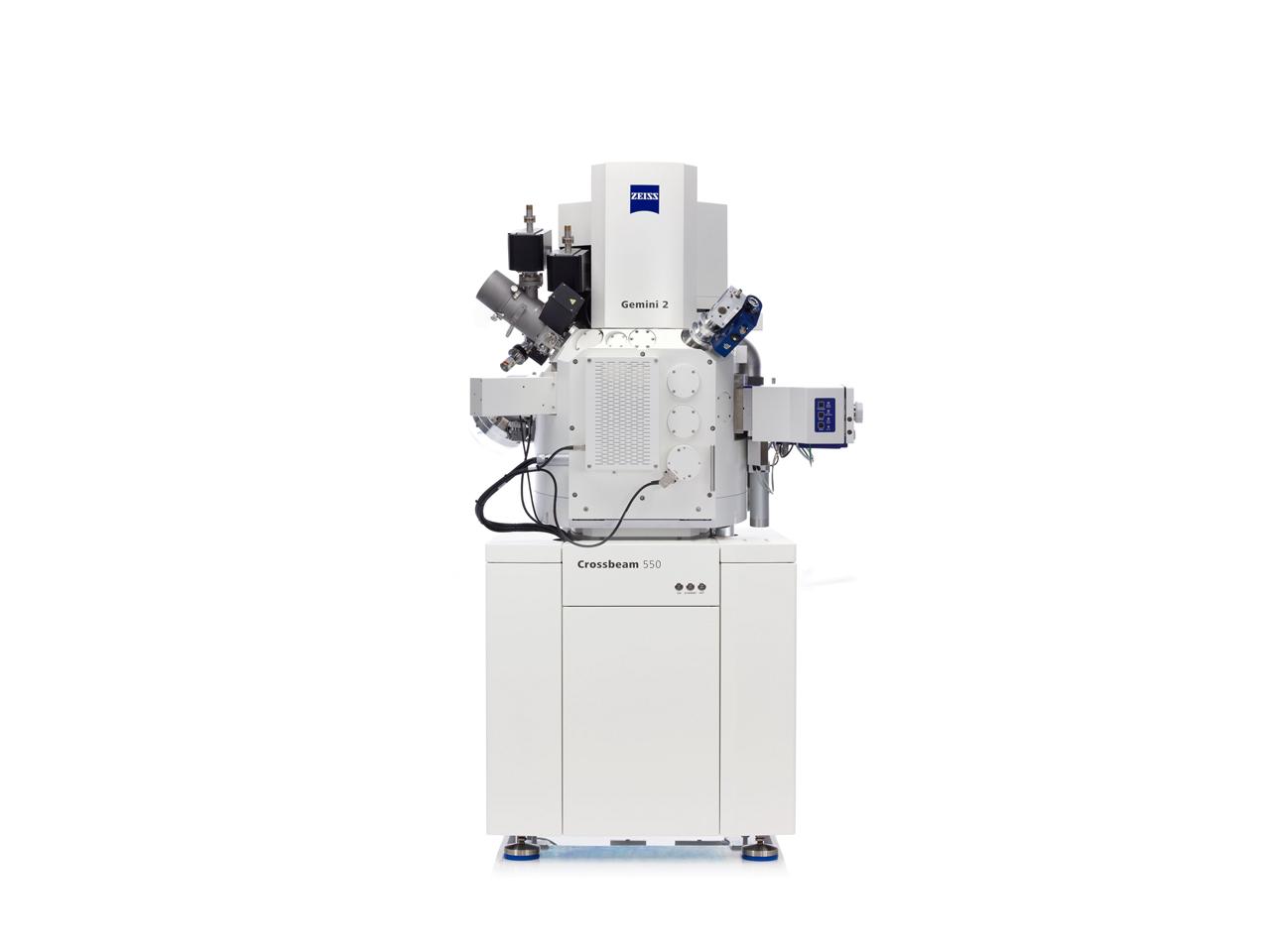
Explore ZEISS GeminiSEM FE-SEM
Nondestructive 3D Imaging of Gyroscope/Accelerometer
In order to identify failures in a semiconductor MEMS device, like an accelerometer, it is important to nondestructively image the sample with sub-micron resolution. ZEISS Versa 3D X-ray microscopes – with its resolution-at-a-distance technology – reveals the nanoscale structures of the MEMS, even within an electronic product.

3D Analysis of Smartphone Gyroscope / Accelerometer
3D Analysis of Smartphone Gyroscope / Accelerometer


High-resolution Image Fine Comb Fin
High-resolution Image Fine Comb Fin


Virtual Slice of Fine Comb Fins
Virtual Slice of Fine Comb Fins
Recommended Products for Multi-dimensional Imaging and Analysis of Semiconductor Packages


Semiconductor Lab Essentials


Microscopy FAQs for Semiconductors
ZEISS offers a variety of microscopy techniques tailored for Semiconductors including:-
ZEISS microscopes, especially the Crossbeam FIB-SEMs, enhance the yield and success of Transmission Electron Microscopy (TEM) lamellae preparation for semiconductor failure analysis through several key features:
High-Resolution Imaging: Essential for Identifying Target Areas and Assessing Sample Quality.
FIB (Focused Ion Beam) Milling: Ga+ focused ion beam – scanning electron microscope (FIB-SEM) for preparing TEM samples with minimal artifacts through simultaneous Imaging while milling and precise end-pointing.
Integrated Analytics: Provides additional insights, such as EDS Elemental Analysis, and Real-Time Feedback during milling to allow quick adjustments and quality enhancement of the lamella.
Automation: Supports semi-automated and automated TEM lamellae prep workflows, optimizing efficiency, yield and success rates.
-
Electron microscope-based techniques like Passive Voltage Contrast (PVC) and Nanoprobing are crucial for defect localization and electrical fault isolation in semiconductor devices.
Passive Voltage Contrast (PVC): Uses SEM to visualize electrical potential differences within semiconductor nanostructures, aiding in defect and fault identification.
Nanoprobing: Utilizes sharp probes for precise electrical measurements on specific nanoscale features that can only be observed under an SEM. Key nanoprobing modes include:
Electron Beam Absorbed Current (EBAC): Measures current from electron absorption, revealing local electrical properties and tracing carrier path.
Electron Beam Induced Current (EBIC): Detects current from electron beam interaction, mapping p-n junctions and electrically active defects.
Electron Beam Induced Resistance Change (EBIRCH): Identifies resistive defects like shorts.
Zeiss GeminiSEM field-emission SEMs allow for seamless integration of imaging and nanoprobing, enabling real-time observation of the electrical characteristics of the device while simultaneously visualizing its structure.
Explore ZEISS GeminiSEM FE-SEM
To learn more about electrical defect localization inside an SEM and Passive Voltage Contrast, please listen to our recent webinar.
-
Nanoscale tomography provides high-resolution, three-dimensional imaging of semiconductor structures, allowing for detailed visualization of internal features and defects. This technique enables precise identification and localization of faults, such as voids, inclusions, and interface irregularities, which are critical for understanding failure mechanisms and improving device reliability.
By reconstructing the 3D architecture of semiconductor devices, nanoscale tomography in a focused ion beam scanning electron microscope (FIB-SEM) facilitates a comprehensive analysis of complex structures, aiding in the development and optimization of advanced semiconductor technologies. True z-depth monitoring with high nm-scale resolution, live imaging while milling, isotropic voxels and integrated analytics are few key features to obtain most accurate 3D reconstruction of the complex structure.


